JSM-IT210 SEM
Manufacturer: JEOL USA, Inc.
SKU: JSM-IT210
Description
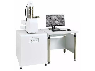
The JSM-IT210 is a scanning electron microscope from JEOL's InTouchScope series. It is a compact system incorporating automated functions for ease of operation. The electron source is a tungsten filament. In high vacuum mode, the resolution is specified as 3.0 nm at 30 kV; in low vacuum mode, using a backscattered electron detector, it is 4.0 nm at 30 kV. The accelerating voltage range is 3 to 30 kV, with probe current adjustable from 1 pA to 1 µA. The motorized stage accommodates specimens up to 150 mm in diameter and 53 mm in height. Operational features include a guided specimen exchange mode, automatic alignment, focus, and stigmation correction. An integrated optical camera (Zeromag) aids in navigation and provides a seamless transition to SEM imaging. The system employs a high-sensitivity quadrant backscattered electron detector capable of live 3D surface reconstruction. Analytical models are available with a fully embedded energy-dispersive X-ray spectroscopy (EDS) system for real-time elemental analysis and mapping. Additional automation includes functions for creating large-area image montages and programmed multi-location imaging.
Specifications
| Item | JSM-IT210 SEM |
| Company | JEOL USA, Inc. |
| Catalog Number | JSM-IT210 |
| Quantity | EA |
| Resolution | High vacuum mode: 3.0 nm at 30 kV Low vacuum mode: 4.0 nm at 30 kV (using Backscattered Electron Detector). |
| Specimen Size | 150 mm diameter x 53 mm height |
| Probe Current | 1 pA to 1 µA |
| Accelerating Voltage | 3 to 30 kV |
| Magnification | Direct magnification: ×5 to ×300,000 (print size of 128 mm × 96 mm) Display magnification: ×14 to ×839,724 (display size of 358 mm × 269 mm) |
| Detector(s) | Small area EDS detector |
| Applications | Compact stationary scanning electron microscope, embedded EDS, live analysis, heat-sensitive specimens, element maps |
Vendors & Pricing
No vendors listed yet
Vendor pricing will appear here once available.