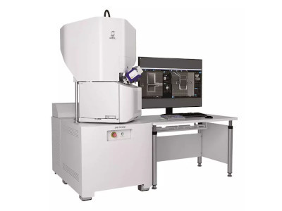
JIB-PS500i FIB-SEM
Manufacturer: JEOL USA, Inc.
SKU: JIB-PS500i
Description
The JIB-PS500i is a combined focused ion beam and scanning electron microscope (FIB-SEM) system designed for materials science and semiconductor applications. It integrates sample preparation, high-resolution imaging, and analytical capabilities. The SEM column delivers a resolution of 0.7 nm at 15 kV and 1.0 nm at 1 kV when using the beam deceleration (BD) mode. The FIB column provides a resolution of 3 nm at 30 kV and supports ion currents up to 100 nA for efficient large-area milling. The system includes multiple detectors: a standard secondary electron detector (SED), an upper electron detector (UED), and an in-lens backscattered electron detector (iBED). A key feature is a large, 5-axis eucentric motorized stage within an accessible chamber, accommodating sizable samples. The instrument is engineered for performance at low accelerating voltages, operating down to 0.5 kV, which is beneficial for imaging beam-sensitive materials. For transmission electron microscopy (TEM) sample preparation, it can produce lamellae thinner than 30 nm and includes a retractable STEM detector for in-situ quality assessment. A workflow termed 'TEM-Linkage' facilitates the transfer of prepared samples directly to a TEM using compatible holders.
Specifications
| Item | JIB-PS500i FIB-SEM |
| Company | JEOL USA, Inc. |
| Catalog Number | JIB-PS500i |
| Quantity | EA |
| Resolution | SEM : 0.7 nm (15 kV) ; 1.4 nm (1 kV); 1.0 nm (1 kV, BD mode) FIB:3 nm (at 30 kV) |
| Detector(s) | Secondary electron detector (SED), Upper electron detector (UED), In-lens backscattered electron detector (iBED) |
| Accelerating Voltage | 0.5 to 30 kV |
| Magnification | SEM: ×50 to ×1,000,000 (STD mode); ×1,000 to ×1,000,000 (UHR mode); ×10 to ×19,000 (LDF mode) (128 mm × 96 mm print size) FIB:×50 to ×300,000 |
| Lens | Power stabilization lens (Objective lens) |
Vendors & Pricing
No vendors listed yet
Vendor pricing will appear here once available.