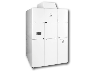
JEM-ACE200F High Throughput Analytical Electron Microscope
Manufacturer: JEOL USA, Inc.
SKU: JEM-ACE200F
Description
The JEM-ACE200F is a scanning/transmission electron microscope (S/TEM) engineered for automated, high-volume analysis, particularly suited for semiconductor research and fabrication. It is designed to perform unattended operation through pre-programmed measurement recipes, enabling consistent morphological inspection, critical dimension metrology, and elemental mapping. The instrument achieves a TEM resolution of 0.10 nm at 200 kV. When equipped with an optional STEM spherical aberration (Cs) corrector, it provides a STEM resolution of 0.10 nm and a high-angle annular dark-field (HAADF) resolution as fine as 63 pm using frame accumulation techniques. Standard detection includes dual energy-dispersive X-ray spectroscopy (EDS) detectors utilizing silicon drift diode (SDD) technology for rapid chemical analysis. The specimen stage offers precise movement with ranges of ±1.0 mm in X and Y and ±0.2 mm in Z. Tilting capabilities vary by holder, with a dual-axis holder providing ±20° and ±25° tilt and a high-tilt holder enabling up to ±80° tilt. Based on the established ARM200F and F2 platforms, this model emphasizes operational stability and measurement repeatability for industrial applications.
Specifications
| Item | JEM-ACE200F High Throughput Analytical Electron Microscope |
| Company | JEOL USA, Inc. |
| Catalog Number | JEM-ACE200F |
| Quantity | EA |
| Resolution | TEM Resolution: 0.10 nm (200 kV). STEM Resolution: 0.10 nm (200 kV, with STEM Cs corrector). STEM-HAADF Resolution: 73 pm on GaN (single frame) or 63 pm (frame accumulation). |
| Detector(s) | Dual EDS detector with SDD technology. |
| Movable Dimensions | X,Y ±1.0 mm, Z ±0.2 mm. |
| Angles | TX/TY (dual-axis holder) ±20°/±25°, TX (high-tilt holder) ±80°. |
| Accelerating Voltage | 60kV to 200kV (80 kV, 200 kV; standard, Other voltages: option) |
Vendors & Pricing
No vendors listed yet
Vendor pricing will appear here once available.