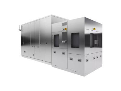
JBX-A9 Electron Beam Lithography System
Manufacturer: JEOL USA, Inc.
SKU: JBX-A9
Description
The JBX-A9 is an electron beam lithography system from JEOL designed for high-precision direct writing on large substrates. It features a maximum scanning speed of 200 MHz and a standard accelerating voltage of 100 kV. The system can handle large sample formats, including 300 mm wafers and 9-inch masks. It offers a sensitivity specification of 1000 µm. The design incorporates JEOL's electron optics for stability and is built with throughput and precision as key objectives. Options include a FOUP (Front-Opening Unified Pod) system for automated handling and in-line connectivity to other process tools like coaters and developers. The system also emphasizes lower power consumption and user-friendly operation for personnel with varying levels of experience.
Specifications
| Item | JBX-A9 Electron Beam Lithography System |
| Company | JEOL USA, Inc. |
| Catalog Number | JBX-A9 |
| Quantity | EA |
| Sensitivity | 1000 µm |
| Scanning Speed | Max. 200 MHz |
| Sample Size | 300 Wafer; 9 inch Mask |
| Accelerating Voltage | 100 kV |
| Dimensions | 7.4 m × 5.3 m × 2.7 m (H) |
| Resolution | Stage Positioning Resolution: 0.15 nm |
| Field Size | Max. 1000 µm |
| Power Consumption | 5 kVA |
Vendors & Pricing
No vendors listed yet
Vendor pricing will appear here once available.