JBX-8100FS
Manufacturer: JEOL USA, Inc.
SKU: JBX-8100FS
Description
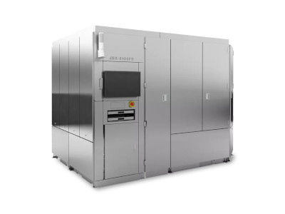
The JEOL JBX-8100FS is a direct-write electron beam lithography system built for high-resolution patterning with improved throughput. It utilizes a spot beam and a vector scan, step-and-repeat method. The standard accelerating voltage is 100 kV, with optional voltages of 200 kV, 130 kV, 50 kV, and 25 kV available. It supports a maximum scanning speed of 125 MHz. The system can accommodate wafers up to 200 mm in diameter, masks up to 6 inches, and micro samples of any size. Key operational features include a selectable field size, with a 100 µm x 100 µm field for high-resolution mode and a 1000 µm x 1000 µm field for high-throughput mode. Overlay accuracy is ±9 nm or better in high-resolution mode and ±20 nm or better in high-throughput mode. The system uses a ZrO/W Schottky emitter and features a stage controlled in 0.6 nm steps (with 0.15 nm optional). Its physical dimensions are approximately 4.9 m wide by 3.7 m deep by 2.6 m high. Design goals include a relatively compact footprint, reduced power consumption, and minimized idle time during exposures to increase overall productivity.
Specifications
| Item | JBX-8100FS |
| Company | JEOL USA, Inc. |
| Catalog Number | JBX-8100FS |
| Quantity | EA |
| Voltage | 100 kV (200kV, 130kV, 50 kV, 25 kV optional) |
| Scanning Speed | Max 125 MHz |
| Sample Size | Wafers up to 200 mmf, masks up to 6 inch, and micro sample pieces of any size |
| Dimensions | 4.9 m (W) x 3.7 m (D) x 2.6 m (H) |
| Method | Spot beam, vector scan, step and repeat |
| Field Size | 100 µm × 100 µm (high resolution mode) 1000 µm × 1000 µm (high throughput mode) |
Vendors & Pricing
No vendors listed yet
Vendor pricing will appear here once available.